Wemos TTGO ESP8266 with 0.91" OLED
I have been looking for an ESP8266 board that has voltage converters like a NodeMCU but is much smaller and space saving. Background is my current project “fridge-kola” to control a wine fridge as an IoT device via my smart home and to read out its state. The TTGO board with integrated OLED display is perfect for my requirements. It has exactly the right size to be placed in the handle of the fridge and offers all necessary interfaces to read my NTC temperature sensor, control the cooling circuit control and the interior lighting. By the way, the board also works with ESPHome without any problems.
Specifications⌗
| MCU | ESPRESSIF-ESP8266EX |
|---|---|
| Flash Size | 4Mb |
| HW Buttons | Reset / Flash |
| Display | 0.91-inch 128*32 monochrome OLED |
| PWR LED | red |
| USB to TTL | CP2102 |
| Clock | 26MHz crystal oscillator |
| Voltage | 3.3V - 7V |
| Avg. Current | ~70mA |
| Temperature | -40℃ ~ 90℃ |
| Board Size | 50.86mm * 18.2mm * 6.96mm |
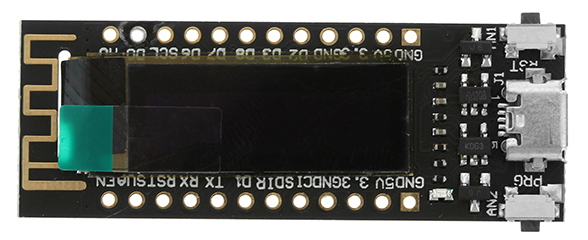
Front View⌗
In addition to the OLED display, two hardware buttons for resetting and flashing the ESP8266 and the micro-USB port are located on the front.
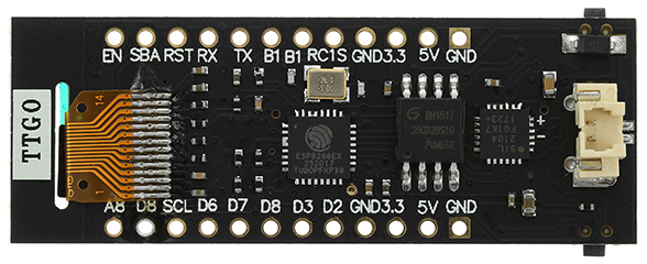
Back View⌗
On the backside there is - unshielded - the ESP8266 chip and a connector for a battery. There are reports about poor WIFI performance in relevant Internet communities. I assume that this is due to the positioning of the antenna behind the flex cable, as well as the lack of shielding of the microcontroller.
Board Layout⌗
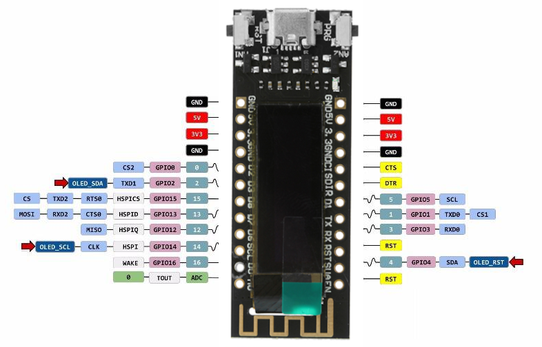
The following pins are occupied by the display:
| OLED | Board |
|---|---|
| SDA | D4 / GPIO2 |
| SCL | D5 / GPIO14 |
| RST | D2 / GPIO4 |
Code Example⌗
// This example of the Adafruit_SSD1306 library worked for me.
// I only modified initialising Wire with the appropriate I2C pins.

...
#define OLED_SDA 2
#define OLED_SCL 14
#define OLED_RST 4
...
Wire.begin( OLED_SDA, OLED_SCL);
...
Interface Pin Function of OLED (WEO012832)⌗
| No. | Symbol | Function |
|---|---|---|
| 1 | C2P | Positive terminal of the flying inverting capacitor |
| 2 | C2N | Negative terminal of the flying boost capacitor |
| 3 | C1P | The charge-pump capacitors are required between the terminals |
| 4 | C1N | They must be floated when the converter is not used |
| 5 | VBAT | Power supply for DC/DC converter circuit. This is the power supply pin for the internal buffer of the DC/DC voltage converter. It must be connected to external source when the converter is used. It should be connected to VDD when the converter is not used. |
| 6 | NC | No connection |
| 7 | VSS | Ground of logic circuit |
| 8 | VDD | Power supply for logic circuit |
| 9 | RES | Power Reset for Controller and Driver. When the pin is low, initialization of the chip is executed |
| 10 | SCL | I2C mode is selected, D2, D1 should be tied together and serve as SDA-out, SDA-in in application and D0 is the serial clock input, SCL. |
| 11 | SDA | - |
| 12 | IREF | Current Reference for Brightness Adjustment. This pin is segment current reference pin. A resistor should be connected between this pin and VSS. Set the current lower than 12.5μA. |
| 13 | VCOMH | Voltage Output High Level for COM Signal. This pin is the input pin for the voltage output high level for COM signals. A capacitor should be connected between this pin and VSS. |
| 14 | VCC | Power Supply for OEL Panel. This is the most positive voltage supply pin of the chip. A stabilization capacitor should be connected between this pin and VSS when the converter is used. It must be connected to external source when the converter is not used. |